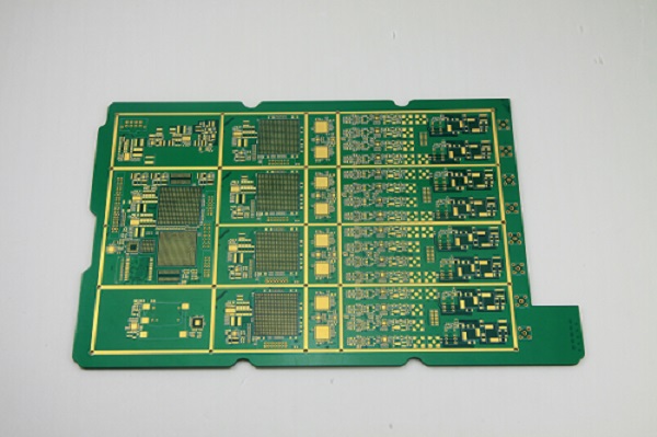
Become an important part of PCB design. Simply put, each hole in the PCB can be called a via. From the perspective of function, the vias can be divided into two types: one is used as an electrical connection between layers; the other is used for fixing or positioning of the device. In terms of process, these vias are generally divided into three categories, namely, Blind Via, Buried Via, and Through Via.

The blind vias are located on the top and bottom surfaces of the printed circuit board and have a depth for the connection of the surface lines to the underlying inner traces, which typically do not exceed a certain ratio (aperture). A buried via is a connection hole located in the inner layer of a printed circuit board that does not extend to the surface of the board. The buried hole is located in the inner layer of the circuit board, and is completed by a through hole forming process before lamination, and several inner layers may be overlapped during the hole forming process. The third type of hole becomes a through hole that passes through the entire circuit board and can be used to achieve internal interconnection or mounting of the component. Since the vias are easier to implement in the process and lower in cost, most printed circuit boards use it without the need for two other vias. From a design point of view, a via is mainly composed of two parts, one is the drill hole (Drill Hole), and the other is the pad area around the drill hole. The size of these two parts determines the size of the vias.
Obviously, when designing high-speed and high-density PCBs, board designers always want the smaller the holes, the more wiring space can be left on the PCB. The smaller the vias, the smaller the parasitic capacitance. More suitable for high speed circuits. However, the reduction in the size of the hole brings about an increase in cost, and the size of the via hole cannot be infinitely reduced. It is limited by the process technology such as Drill and Plating. The smaller the hole, the longer it takes for the hole to be drilled and the easier it is to deviate from the center position. At the current level of PCB fabrication technology, when the ratio of the thickness of the PCB substrate to the aperture (ie, the aspect ratio) exceeds 10, uniform copper plating of the hole walls cannot be ensured, and the thickness of the copper layer is not uniform, especially in the middle of the plating layer. Loose and too thin coatings can seriously affect the fatigue life of the hole.
